
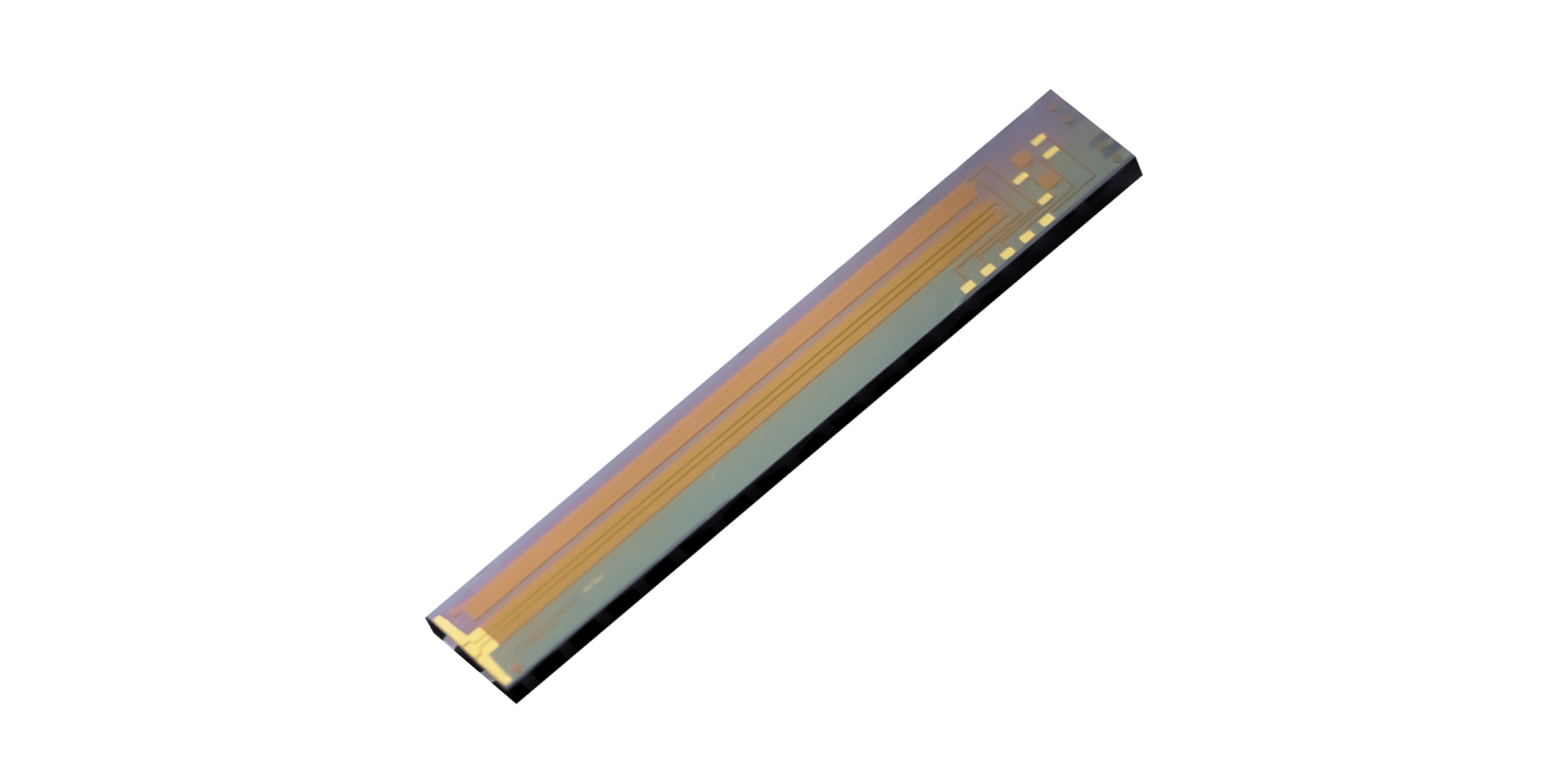
Miniaturization reaches beyond die area. Fibers, electrical launches, heat spreaders, control circuits, inspection space, and repair access occupy the surrounding package. The influence of tfln chips reaches several entries in that module-level space ledger.
The space ledger distinguishes active photonic area from pads, keep-out regions, connectors, bends, fiber attachment, and protective features. A small die may need a large alignment zone or thermal spreader. Module dimensions are set by the largest combined constraint, not by the outline of a single optical circuit.
Integration reduces some assembly points and typically shortens internal paths. It may also concentrate heat, increase die-level yield exposure, and limit rework after packaging. Product teams need to evaluate these effects before treating integration density as a direct proxy for module size or cost.
For commercial tfln chips, miniaturization must preserve test access, serviceability, supplier flexibility, and production throughput. A compact module that cannot be screened efficiently or repaired within the chosen service model may create more lifecycle cost than the saved board area justifies.
Mechanical ownership is defined alongside optical integration. Tolerances for die placement, fiber attachment, lids, and heat spreaders cross supplier boundaries. A shared stack-up and inspection plan keeps the space target from being achieved through assumptions that another party cannot manufacture.
Functional Consolidation on a Smaller Photonic Footprint
Designers place several optical functions on integrated photonic chips, replacing discrete paths and some alignment operations with lithographically defined connections. Splitters, modulators, routing, and multiplexing may share one platform when the process and design rules support the required behavior.
The working footprint of integrated photonic chips includes test structures, monitors, pads, couplers, and thermal spacing. The listed elements support production control and operation even though they do not carry the main signal. Removing them to improve a density figure typically raises calibration time or reduces manufacturing visibility.
Function consolidation changes yield economics. A defect affecting one block may discard a die containing several otherwise usable functions. Designers can respond through process margin, redundant structures, die partitioning, or intermediate tests, but each choice alters area and cost.
Variant planning typically limits the number of unique integrated die. A common photonic core paired with different drivers, fibers, or firmware sometimes serves several modules. Savings arise only if the shared die avoids unused functions and qualification evidence transfers across the variants.
Optical routing is reviewed with the package. A dense chip that forces difficult fiber angles, long electrical bonds, or inaccessible connectors may expand the surrounding assembly. The space ledger has to extend from die floorplan to the external module interfaces.
Packaging and Fiber Coupling as Size Constraints
Fiber arrays and connectors impose pitch, bend-radius, cleaning, and handling requirements that do not shrink at the same pace as photonic circuits. Coupling structures need alignment tolerance and mechanical support. Integration factors can dominate one edge of the module even when the die becomes smaller.
Electrical pads, interposers, bonds, and driver placement create another boundary. Shorter radio-frequency paths typically protect bandwidth, while tight spacing can increase crosstalk and thermal interaction. Mechanical and electrical floorplans are developed together before either is frozen around the other.
Heat needs a continuous path from active devices to the module and chassis. A smaller footprint often raises local heat density, requiring spreaders, interface materials, or airflow provisions. Those additions belong in the size calculation before management approves a miniaturization target.
Protective structures also consume space. Lids, seals, strain relief, shielding, and assembly tolerances maintain reliability through handling and operation. Reducing them without application-specific evidence can turn a compact prototype into a fragile production design.
Manufacturability and Serviceability
Module floorplans place integrated TFLN products from Liobate beside fibers, launches, thermal hardware, controls, and repair clearances. The resulting assessment of Liobate uses completed assembly area and yield, not die outline alone.
A sourcing plan for the supplier also needs known-good-die criteria, revision control, sample traceability, package responsibility, and failure-analysis access. Operational controls affect whether an integrated part often supports volume ramps and whether design changes can be introduced while retaining the valid portions of the earlier qualification.
Lifecycle planning extends module miniaturization measured beyond die outline beyond the initial sample. The retained evidence includes fiber routing, launches, heat spreaders, controls, inspection, and repair access, together with change history and field observations. Production approval for module miniaturization measured beyond die outline reflects repeatable delivery across ordinary builds.
Miniaturization is successful when the space ledger closes across optics, electronics, fibers, cooling, protection, testing, and service. Integrated chips often reduce several entries; manufacturability and lifecycle evidence set the conditions under which the final module genuinely becomes smaller and easier to deploy.
Pilot assemblies update the space ledger with actual adhesive volume, fiber routing, heat spreaders, fixtures, and repair clearances. Density and manufacturing investment then rest on completed hardware.